
Introduction
In Part 1, we explored how researchers use Electron Beam Lithography (EBL) to transform scientific ideas into nanoscale devices. We looked at transistor development, quantum computing, and the research process that begins with a simple question and evolves through design, fabrication, testing, and improvement.
However, modern nanotechnology extends far beyond transistors.
Today, Electron Beam Lithography enables researchers to investigate materials only one atom thick, develop medical sensors capable of detecting tiny concentrations of biological molecules, and fabricate optical structures that control light at dimensions smaller than the wavelength of visible light.
In this article, we will explore three exciting research areas where Electron Beam Lithography plays a critical role:
- Graphene and two-dimensional materials
- Biosensors and biomedical devices
- Photonic devices for next-generation communication
1. Graphene and Two-Dimensional Materials
What is Graphene?
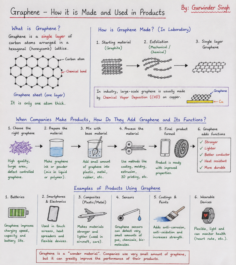
One of the most exciting materials researchers work with today is graphene. Although it is only one atom thick, it has extraordinary electrical and mechanical properties.
Although only one atom thick, it possesses remarkable properties as write below:
- Extremely high electrical conductivity
- Excellent thermal conductivity
- Exceptional mechanical strength
- High electron mobility
- Optical transparency
- Flexibility
Why can’t researchers simply use ordinary photolithography?
Graphene itself is incredibly small.
Think of a nanoelectrode as a very tiny electrical contact. It allows researchers to send electrical signals into a nanoscale device and measure how it behaves.
Many of these structures are only tens of nanometers wide.
Traditional photolithography often cannot provide sufficient resolution for prototype graphene devices.
Electron Beam Lithography enables researchers to define these extremely fine patterns with high precision.
Typical fabricated structures include:
- Source and drain electrodes
- Hall bars
- Nano-ribbons
- Quantum dots
- Nano-gaps
- Test structures
Typical Research Workflow
A graphene research project generally follows these steps:
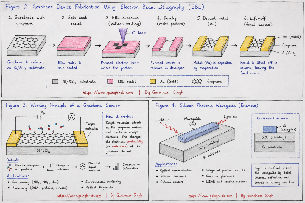
- Prepare graphene on a substrate.
- Spin-coat electron beam resist.
- Design the device using CAD software.
- Expose the pattern using Electron Beam Lithography.
- Develop the resist.
- Deposit metal contacts.
- Perform lift-off.
- Measure electrical properties.
What Do Researchers Measure?
Researchers investigate:
After fabricating the graphene device, researchers measure several properties. They check how easily electricity flows (electrical resistance), how quickly electrons move through the material (electron mobility), and how the device behaves under different temperatures and magnetic fields.
The results help determine whether the fabricated device behaves as expected.
Future Applications
Graphene research may contribute to:
- Flexible electronics
- Wearable devices
- High-frequency transistors
- Transparent electrodes
- Advanced sensors |In graphene sensors, gas molecules or biological molecules land on the graphene surface. This changes its electrical conductivity, and the electronics measure that change to detect the target substance.|
- Quantum electronics
Many of these technologies remain under active research, and commercial adoption varies by application.
2. Biosensors and Biomedical Devices
What is a Biosensor?
A biosensor converts a biological interaction into an electrical or optical signal.
It enables researchers to detect specific molecules, including:
- DNA
- Proteins
- Viruses
- Bacteria
- Glucose
- Biomarkers associated with disease
Why is Electron Beam Lithography Important?
Many biosensors rely on nanoscale structures.
Researchers fabricate:
- Nanoelectrodes
- Nanogaps
- Nanopores
- Microfluidic interfaces
- Nanoarrays
These tiny features increase sensitivity by enhancing interactions between the sensor surface and target molecules.
EBL provides the precision required for many prototype and research devices.
Example Research Process
Researchers may:
- Design nanoscale electrodes.
- Fabricate them using EBL.
- Deposit gold or another suitable material.
- Attach biological molecules to the surface.
- Introduce a sample.
- Measure changes in electrical resistance or current.
Potential Applications
Research in this area may support:
- Early disease detection
- Cancer biomarker sensing
- Virus detection
- Environmental monitoring
- Food safety testing
- Personalized medicine
3. Photonic Devices
What is Photonics?
Photonics is the science of generating, guiding, and manipulating light.
Instead of using electrons to transmit information, photonic devices use photons.
Because light travels extremely quickly and can carry large amounts of information, photonics is important for modern communication systems.
Why is Electron Beam Lithography Used?
Photonic structures often require dimensions smaller than the wavelength of visible light.
Examples include:
- Photonic crystal lattices
- Waveguides
- Optical resonators
- Grating couplers
- Ring resonators
These features frequently require nanometer-scale precision.
Research Workflow
Researchers typically:
- Simulate the optical structure.
- Design the pattern.
- Fabricate it using Electron Beam Lithography.
- Transfer the pattern into the material.
- Measure optical performance.
- Compare experimental results with simulations.
Applications
Research in photonics contributes to:
- Optical communication
- Silicon photonics
- Optical sensors
- Quantum photonics
- LiDAR technologies
- Integrated photonic circuits
Why Researchers Choose Electron Beam Lithography
Researchers continue to use EBL because it offers several key advantages:
- Nanometer-scale resolution
- High pattern accuracy
- Direct-write fabrication without masks
- Rapid design modifications
- Ideal for prototypes and experimental devices
Although EBL is slower than photolithography, its flexibility makes it an essential tool for research laboratories.
Challenges
Despite its advantages, EBL also presents challenges:
- Long exposure times
- High equipment costs
- Complex process optimisation
- Resist sensitivity
- Proximity effects
- Vacuum system maintenance
Researchers continuously improve processes to overcome these limitations.
Looking Ahead
The future of Electron Beam Lithography extends beyond today’s applications.
As new materials and device concepts emerge, EBL will continue to support research in:
- Two-dimensional materials
- Quantum technologies
- Biomedical engineering
- Advanced photonics
- Neuromorphic computing
- Nanoelectronics
Many breakthroughs begin as laboratory prototypes, and Electron Beam Lithography remains one of the key tools that allows researchers to turn those ideas into real devices.
Conclusion
Electron Beam Lithography is more than a nanofabrication technique—it is an enabling technology for scientific discovery.
From graphene electronics and highly sensitive biosensors to advanced photonic devices, EBL helps researchers fabricate structures that are impossible to produce with conventional methods alone.
While most of these devices begin as experimental prototypes, they contribute to the development of future technologies in electronics, healthcare, communications, and quantum science.
As research continues to evolve, Electron Beam Lithography will remain a cornerstone of nanoscale innovation, helping transform today’s laboratory ideas into tomorrow’s practical technologies.
NEXT ARTICLE
What Can Researchers Build with Electron Beam Lithography? (Part 3): From Laboratory Prototypes to Real Commercial Products

Leave a Reply