Category ELECTRON BEAM LITHOGRAPHY

What Can Researchers Build with Electron Beam Lithography? (Part 2): Graphene, Biosensors & Photonic Devices

Introduction In Part 1, we explored how researchers use Electron Beam Lithography (EBL) to transform scientific ideas into nanoscale devices. We looked at transistor development, quantum computing, and the research process that begins with a simple question and evolves through…
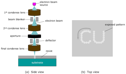
Electron Beam Lithography (EBL) is a cutting-edge technique used to create extremely fine patterns required in the manufacture of semiconductor devices, nanotechnology, and other fields that demand high precision.

Unlike traditional photolithography that uses light, EBL employs a focused electron beam to draw custom shapes on a surface coated with an electron-sensitive resist. How Does EBL Work?Coating the Substrate: A thin layer of electron-sensitive resist material is applied to…