
When I first started learning about positioning in an EBL system, I thought alignment marks were mainly used to tell the machine where the wafer was.
But then I had another question.
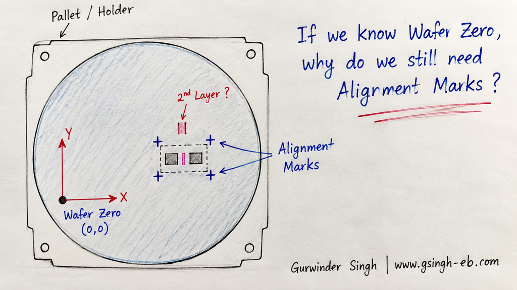
If the wafer is already mounted on a pallet or holder, and the EBL system has a wafer-zero position, don’t we already know where the wafer is?
If we know wafer zero, we can use X-Y coordinates and move to different positions on the wafer quite easily.
So why do we still need alignment marks?
This question helped me understand that knowing where the wafer is and aligning a new pattern to an existing structure are actually two different things.
First, What Do I Mean by Wafer Zero?
Let’s start with a simple case.
We have a wafer mounted on a pallet or sample holder. The machine needs some reference from which other positions can be defined.
We can think of wafer zero as a reference point for the wafer coordinate system.
For example, once the reference has been established, a position might be described as:
X = 10 mm, Y = 5 mm
Now the machine has a way to move to that location.
This makes wafer navigation much easier because we don’t have to manually search the whole wafer every time we want to expose a pattern.
The exact way wafer zero is established can depend on the EBL system and sample setup, but the basic idea is simple:
We need a known reference before other X-Y positions become meaningful.
Then Why Do We Need Alignment Marks?
This was the part that initially confused me.
If wafer zero already gives us a coordinate reference, shouldn’t that be enough?
For some exposures, it may be enough.
Imagine I have a fresh resist-coated wafer and I just want to write a new pattern at a certain location.
I establish the wafer reference, move to the required X-Y position and expose the pattern.
There may be no existing nanoscale structure that my new pattern has to match exactly.
But now imagine something different.
I have already fabricated the first layer of a device.
Later, I coat the wafer again and want to expose a second layer.
This time I don’t only need to know:
“Where am I on the wafer?”
I need to know:
“Where exactly is my first-layer structure, so that my second-layer pattern can be placed correctly relative to it?”
That is a different problem.
A Simple Device Example
Suppose my first fabrication step creates two structures.
For simplicity, let’s call them source and drain:
SOURCE                         DRAIN

████████                       ████████
Now imagine that in another lithography step I want to place a small gate between them.
My GDSII design might look perfect:
SOURCE          GATE           DRAIN

████████          │            ████████
                  │
Inside the computer, there is no problem.
The gate coordinates are exactly where I designed them.
But the real wafer has gone through fabrication.
It may have been removed from the EBL system, developed, processed, cleaned, coated again and then loaded back onto the system.
Even if the wafer-zero reference lets us return very close to the correct area, the question for a high-accuracy multilayer process becomes:
Is my second-layer pattern positioned correctly relative to the first layer?
This is where alignment marks become important.
What Is an Alignment Mark?
An alignment mark is a structure intentionally placed on the sample so that it can be used as a physical reference during later alignment.
It may look like a cross, box or another shape depending on the process and equipment.
For example:
      +                         +

             DEVICE

      +                         +
The important thing is not just the shape.
We know where these marks are supposed to be according to our design, and the system can determine their actual positions on the physical sample using its alignment procedure.
Now we have something that connects the existing fabricated layer with the new pattern we want to expose.
Wafer Zero and Alignment Marks Are Solving Different Problems
This is the easiest way I found to understand it.
Wafer zero asks:
“Where is my wafer coordinate reference?”
It helps establish the coordinate system and navigate around the wafer.
Alignment asks:
“Where is my existing pattern relative to the new pattern I want to write?”
It becomes especially important when we need accurate layer-to-layer registration.
So I don’t think of wafer zero and alignment marks as competing methods.
They can be parts of the same positioning process, but they are doing different jobs.
A simple way to remember it is:
Wafer zero → wafer-level reference
Alignment marks → pattern/layer-level reference
The exact implementation and accuracy will depend on the EBL system and process.
Why Can’t We Just Make Wafer Zero Perfect?
This was my next question.
If wafer zero is useful, why not make it so accurate that alignment marks are unnecessary?
The problem is that the physical wafer is not permanently fixed to one perfect coordinate system through every fabrication step.
The wafer can be unloaded and loaded again.
Its mounting position can change slightly.
There can be a small rotation.
The sample may also go through several processing steps before returning for another exposure.
At a large scale, these differences might look extremely small.
But EBL is often being used to fabricate structures measured in nanometers.
That changes how we think about positioning errors.
For example, if a feature is several millimeters wide, a tiny positioning difference may not matter much.
But if two nanoscale layers need tight overlay, that same positioning difference can become important.
So simply knowing the general wafer position is not always the same as knowing the exact position of an existing nanostructure.
What Does the Machine Learn From Alignment Marks?
Let’s imagine that the GDSII file says an alignment mark should be at a certain X-Y coordinate.
The machine searches around the expected location and detects the actual mark using the alignment procedure supported by that system.
Now we have two pieces of information:
Expected mark position from the design
and
Measured mark position on the real wafer.
If they don’t match perfectly, that tells us something about the relationship between the design coordinate system and the actual sample.
Using suitable alignment marks and procedures, the system can account for positioning differences such as translation and rotation. More advanced corrections can depend on the equipment and alignment method.
I think this is much easier to understand when we stop thinking of alignment marks as just “crosses on the wafer.”
They are really reference points that help connect the digital design to the physical structures already fabricated on the sample.
Wafer Zero Does Not Mean the Whole Wafer Is Being Exposed
There is another distinction worth making because it connects to something I was confused about earlier.
Suppose my writing field is 600 µm.
That does not mean wafer zero creates a 600 × 600 µm exposed area.
And it doesn’t mean the whole field receives the electron dose.
These are separate concepts.
Wafer zero relates to positioning/reference.
Writing field relates to the area that can be addressed under a particular writing condition before stage repositioning is needed.
GDSII tells us the geometry that should be written.
Dose tells us how much charge should be delivered per exposed area.
Keeping these ideas separate makes the whole EBL process much easier to understand.
What Happens If Alignment Is Wrong?
Imagine that the gate in our previous example is supposed to be exactly here:
SOURCE          GATE          DRAIN

████████          │           ████████
                  │
But because of an overlay error, we get:
SOURCE              GATE      DRAIN

████████               │      ████████
                       │
The electron beam may have written the gate pattern correctly in terms of its shape and size.
The dose might also have been correct.
The beam could have been properly focused.
But the pattern was written at the wrong position relative to the first layer.
This made me realize something important:
Resolution and positioning accuracy are not the same thing.
An EBL system doesn’t only need to make small features.
For many applications, it also needs to place those features correctly.
A Simple Way I Remember the Whole Process
Now I think about positioning like this:
Wafer mounted on pallet/holder
↓
Establish wafer reference / wafer zero
↓
Machine has a wafer coordinate system
↓
Move close to the required device area
↓
If precise overlay to an existing layer is required, use alignment references
↓
Relate the existing physical pattern to the new design
↓
Expose the next GDSII pattern at the required position
This also helped me understand why different EBL jobs can have different alignment requirements.
If I am simply writing a test pattern on a fresh resist-coated substrate, my positioning requirements may be different from a multilayer device where one nanoscale feature has to line up with another.
What I Understood
Initially, I thought:
If we know wafer zero, why do we need alignment marks?
Now I see that I was combining two different questions.
Wafer zero helps answer:
“Where am I on the wafer?”
Alignment marks help answer:
“Where is the structure that I need my next pattern to align with?”
That difference sounds small, but it changed the way I understand EBL positioning.
The GDSII file gives us the digital design.
Wafer zero helps establish a physical coordinate reference.
Alignment marks can then help connect a new exposure to structures that already exist on the real wafer.
So the complete problem is not simply:
Can the electron beam make a 20 nm or 50 nm feature?
We also have to ask:
Can we put that feature where it actually needs to be?
Conclusion
EBL becomes much easier to understand when we separate the different jobs the machine is doing.
GDSII tells us what to write.
Dose tells us how much charge to deliver per exposed area.
Beam current tells us how quickly charge is delivered.
Wafer zero helps establish where we are on the wafer.
Alignment marks help register a new pattern to existing structures when accurate overlay is required.
For me, this was the important point:
Knowing the wafer position is not always the same as knowing the exact position of an existing device layer.

Leave a Reply