
Published on July 5, 2026 GURWINDER SINGH
Introduction
Modern semiconductor devices contain billions of transistors packed into an area no larger than a fingernail. As electronic devices continue to shrink, fabricating structures at the nanometer scale requires technologies capable of extraordinary precision. One of the most important techniques used for this purpose is Electron Beam Lithography (EBL).
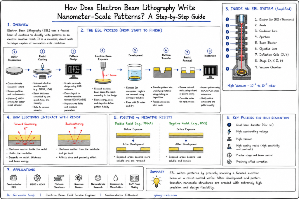
Unlike conventional photolithography, which uses ultraviolet light and photomasks, Electron Beam Lithography uses a highly focused beam of electrons to directly write patterns onto an electron-sensitive resist. This maskless approach provides exceptional flexibility and enables researchers to fabricate structures only a few nanometers wide.
In this article, we will explore how Electron Beam Lithography works, from preparing the wafer to creating the final nanoscale pattern.
What Is Electron Beam Lithography?
Electron Beam Lithography is a direct-write nanofabrication technique in which a focused beam of electrons selectively exposes an electron-sensitive resist deposited on a substrate.
Because the beam is controlled by a computer, engineers can create almost any pattern without manufacturing a new photomask. This makes EBL especially valuable for research laboratories, prototype development, photonics, quantum devices, MEMS, and advanced semiconductor research.
Why Use Electrons Instead of Light?
One of the biggest advantages of EBL is the use of electrons instead of visible or ultraviolet light.
Electrons accelerated to high energies have extremely short wavelengths, allowing them to be focused into spots only a few nanometers in diameter. This enables patterning at resolutions that are difficult for conventional optical lithography to achieve.
However, this increased precision comes at the cost of slower writing speeds, which is why EBL is primarily used for research, prototyping, and specialized manufacturing rather than high-volume chip production.
Step 1 – Wafer Preparation
The fabrication process begins with a thoroughly cleaned substrate, typically a silicon wafer. At the nanometer scale, even microscopic particles, organic contaminants, or a thin layer of moisture can affect pattern quality and reduce fabrication yield. Therefore, maintaining a clean surface is a fundamental requirement before applying the electron beam resist.
To further improve resist adhesion, the wafer often undergoes a dehydration bake. This step removes adsorbed moisture from the wafer surface, creating a more stable interface for the resist coating. Depending on the fabrication process, an adhesion promoter such as HMDS (Hexamethyldisilazane) may also be applied before spin coating to further enhance resist adhesion.
Engineering Note: The dehydration bake is different from the soft bake (prebake) performed after resist coating. The dehydration bake prepares the wafer surface, whereas the soft bake removes residual solvent from the resist layer.
Step 2 – Resist Coating and Soft Bake
After the wafer has been thoroughly cleaned and prepared, an electron-sensitive resist is applied to its surface using a spin coating process. The resist serves as a temporary imaging layer that records the pattern written by the electron beam.
During spin coating, a small volume of liquid resist is dispensed onto the center of the wafer. The wafer is then rotated at high speed, typically between 1,000 and 6,000 rpm, depending on the desired resist thickness and the resist manufacturer’s process recommendations. Centrifugal force spreads the resist uniformly across the wafer, producing a smooth and controlled thin film.
The final resist thickness is influenced by several factors, including:
- Spin speed
- Spin time
- Resist viscosity
- Resist concentration
- Ambient temperature and humidity
Selecting an appropriate resist thickness is an important process consideration. A thinner resist generally provides higher resolution because it reduces electron scattering within the resist, while a thicker resist may be preferred for applications requiring deeper etching or more robust pattern transfer.
Several electron beam resists are commonly used in nanofabrication, including:
| Resist | Type | Typical Applications |
|---|---|---|
| PMMA | Positive | High-resolution research, lift-off processes |
| HSQ | Negative | Ultra-high-resolution nanostructures |
| ZEP-520A | Positive | Higher sensitivity than PMMA |
| CSAR 62 | Positive | High-resolution and high-throughput applications |
After spin coating, the wafer undergoes a soft bake (prebake) to remove residual solvent from the resist and improve film stability before electron beam exposure. This step enhances resist adhesion, reduces process variation, and helps achieve more uniform exposure during lithography.
For many PMMA-based processes, soft-bake temperatures are commonly in the range of 170–180°C for several minutes. However, the optimum baking temperature and duration depend on the resist type, film thickness, and the manufacturer’s recommended process conditions.
Engineering Note: Although soft baking removes solvent from the resist, excessive baking can alter the resist’s chemical properties and affect exposure sensitivity. Therefore, baking conditions should always follow the resist manufacturer’s recommended process.
Step 3 – Pattern Design and Data Preparation
Before electron beam exposure can begin, the desired nanoscale structure must first be designed digitally using Computer-Aided Design (CAD) software. This digital layout serves as the blueprint that defines the geometry, dimensions, and position of every feature to be fabricated on the wafer.
Depending on the application, the design may include:
- Semiconductor devices and test structures
- Nanowires and nanodots
- Photonic crystals and waveguides
- MEMS and NEMS structures
- Quantum devices
- Microfluidic channels
- Alignment marks and calibration patterns
Unlike conventional photolithography, where a photomask contains the circuit pattern, Electron Beam Lithography writes the design directly from the digital layout. This maskless approach allows engineers to rapidly modify or optimize a design without manufacturing a new mask, making EBL highly suitable for research and prototype development.
Once the design is completed, the CAD file is exported into a machine-readable format compatible with the Electron Beam Lithography system. Common layout file formats include GDSII (Graphic Data System II) and OASIS, which store the geometric information required for pattern generation.
Before exposure, the pattern preparation software processes the layout by dividing it into writing fields, assigning exposure parameters, and generating the beam scanning instructions required by the EBL system. In advanced applications, techniques such as proximity effect correction (PEC) may also be applied to compensate for electron scattering and improve pattern accuracy.
Engineering Note: Although the CAD file defines the desired geometry, the Electron Beam Lithography system ultimately converts this information into precise beam movements, exposure doses, and stage positions to accurately reproduce the design on the resist-coated wafer.
Step 4 – Electron Beam Generation
IStep 4 – Electron Beam Generation
At the heart of every Electron Beam Lithography (EBL) system is the electron source, commonly known as the electron gun. Its primary function is to generate a stable and highly focused beam of electrons that can be precisely controlled during the lithography process.
Since electrons can easily collide with air molecules and lose energy, the entire electron column operates under high-vacuum conditions, typically in the range of 10⁻⁵ to 10⁻⁷ Pa (depending on the system design). Maintaining a high vacuum minimizes electron scattering, improves beam stability, and helps protect sensitive components such as the electron source.
Modern EBL systems generally use one of three types of electron sources:
| Electron Source | Principle | Characteristics | Typical Applications |
|---|---|---|---|
| Thermionic Emitter | Electrons are emitted by heating a filament (e.g., tungsten or LaB₆). | Simple, reliable, and relatively inexpensive, but lower brightness and a larger energy spread. | Basic SEMs and older EBL systems |
| Schottky Emitter | Combines moderate heating with a strong electric field to extract electrons. | High brightness, excellent stability, and long operating lifetime. | Modern EBL systems and high-resolution SEMs |
| Field Emission Gun (FEG) | Electrons are extracted from a sharp tip by a very strong electric field. | Extremely high brightness, small source size, and excellent coherence, making it ideal for ultra-high-resolution applications. | Advanced EBL systems, high-performance SEMs, and electron microscopy |
Once emitted, the electrons are accelerated by a high-voltage electric field, typically between 10 kV and 100 kV, depending on the application and the EBL system. Higher accelerating voltages generally reduce electron scattering within the resist and improve beam penetration, although the optimum operating voltage depends on factors such as the resist material, resist thickness, substrate composition, and the required pattern resolution.
The resulting high-energy electron beam is then directed into the electron optical column, where electromagnetic lenses and beam control components shape, focus, and position the beam before it reaches the resist-coated wafer.
Engineering Note: The quality of the electron source has a direct influence on beam brightness, beam stability, spot size, and ultimately the resolution and writing performance of the Electron Beam Lithography system.
Step 5 – Beam Focusing and Deflection
Once the electrons have been generated and accelerated, they must be precisely focused and directed toward the desired location on the wafer. This is achieved through a combination of electron optics, including electromagnetic lenses, apertures, and deflection coils.
Unlike optical systems that use glass lenses to bend light, Electron Beam Lithography systems use electromagnetic lenses to control the trajectory of electrons. These lenses generate magnetic fields that converge the electron beam into an extremely small spot, often only a few nanometers in diameter. The quality of this focused beam directly influences the resolution and accuracy of the fabricated pattern.
To further improve beam quality, apertures are used to limit the beam diameter and remove high-angle electrons that could degrade image quality. Some EBL systems also employ stigmators to correct beam astigmatism, ensuring that the beam remains circular and sharply focused.
Once the beam has been focused, electromagnetic deflection coils rapidly steer it across the writing field according to the digital pattern generated by the control software. These coils can move the beam with nanometer-level precision without requiring any mechanical movement.
However, the beam can only be deflected accurately over a limited writing field. For larger patterns, the motorized precision stage moves the wafer to the next writing field while the electron beam continues exposing the design. Modern EBL systems often use laser interferometer feedback to achieve highly accurate stage positioning and maintain precise alignment between adjacent writing fields.

The combination of high-quality electron optics, fast beam deflection, and precision stage movement enables Electron Beam Lithography systems to reproduce complex nanoscale structures with exceptional placement accuracy.
Engineering Note: Beam spot size, lens alignment, deflection accuracy, stage stability, and vibration control all influence the final pattern quality. Even slight misalignment or mechanical vibration can affect critical dimensions when fabricating features at the nanometer scale.
Step 6 – Pattern Exposure
After the electron beam has been generated, focused, and accurately aligned, the actual lithography process begins. During this stage, the Electron Beam Lithography (EBL) system follows the digital layout generated from the CAD design and selectively exposes the electron-sensitive resist coated on the wafer.
Unlike conventional optical lithography, which transfers an entire pattern through a photomask in a single exposure, Electron Beam Lithography is a direct-write technique. The focused electron beam scans across the wafer and writes the desired pattern point by point with nanometer-scale precision. Because no photomask is required, engineers can easily modify the design by simply updating the digital layout, making EBL an ideal technology for research, prototyping, and low-volume device fabrication.
Depending on the EBL system and application, the beam may follow either a raster scanning strategy, where the entire writing field is scanned line by line, or a vector scanning strategy, where the beam moves only to the regions that require exposure. Vector scanning is generally more efficient for sparse patterns because the beam does not waste time scanning empty areas.
To achieve high pattern accuracy, several exposure parameters must be carefully optimized.
Key Exposure Parameters
1. Beam Current
Beam current determines the number of electrons delivered to the resist per unit time and directly influences the writing speed.
Example:
Imagine painting a wall. A large paint roller covers a large area quickly but is not ideal for painting fine details. A small paintbrush takes longer but produces much finer details. Similarly, a higher beam current increases writing speed, while a lower beam current is often preferred when fabricating extremely small features.
2. Exposure Dose
Exposure dose is the total amount of electron charge delivered to the resist and is commonly expressed in µC/cm².
Example:
Think of taking a photograph. Too little light produces a dark image, while too much light overexposes it. Likewise, if the electron dose is too low, parts of the resist may not develop correctly. If the dose is too high, the exposed features may become wider than intended.
3. Dwell Time
Dwell time is the length of time the electron beam remains at each writing position.
Example:
Imagine focusing sunlight onto a piece of paper using a magnifying glass. Holding the light on one spot for only a brief moment produces little effect, while keeping it there for too long may burn the paper. In Electron Beam Lithography, insufficient dwell time may not expose the resist adequately, whereas excessive dwell time can lead to overexposure.
4. Step Size (Pixel Spacing)
Step size, also called pixel spacing, is the distance between adjacent beam positions during scanning.
Example:
Imagine drawing a circle using individual dots. If the dots are placed very close together, the circle appears smooth and well-defined. If the dots are spaced too far apart, the circle looks jagged and uneven. Similarly, a smaller step size improves edge smoothness and pattern accuracy, while a larger step size increases writing speed but may reduce feature quality.
5. Accelerating Voltage
Accelerating voltage determines the energy of the electrons before they strike the resist.
Example:
Imagine throwing a tennis ball into a stack of cushions. A gently thrown ball stops near the surface, whereas a faster throw penetrates deeper into the cushions. In the same way, higher accelerating voltages give electrons more energy, allowing them to penetrate further into the resist and generally reducing forward scattering. However, the optimum voltage depends on the resist material, substrate, and the desired feature size.
Carefully balancing these parameters is essential for achieving high-resolution patterns with accurate dimensions. In practical Electron Beam Lithography, exposure conditions are optimized through process calibration because every combination of resist, substrate, accelerating voltage, and device geometry behaves differently.
Engineering Note: There is no universal set of exposure parameters that works for every Electron Beam Lithography process. Engineers typically optimize beam current, exposure dose, dwell time, and accelerating voltage through experimental calibration to achieve the desired resolution, pattern fidelity, and fabrication yield.
Step 7 – Resist Development: Making the Invisible Pattern Visible
After the electron beam finishes writing the pattern, something surprising happens…
You still can’t see anything.
Although the electron beam has changed the chemical structure of the resist, the pattern remains invisible to the human eye. At this stage, the wafer looks almost exactly the same as it did before exposure.
So how does the hidden pattern become visible?
The answer is resist development.
During this step, the wafer is placed into a special chemical solution called a developer. The developer reacts only with the regions whose chemical properties have changed during electron beam exposure. As a result, the hidden pattern gradually appears on the wafer.
Think of it like developing an old photographic film. The image already exists after exposure, but it only becomes visible after being placed in the developer solution.
Positive Resist
In a positive resist, such as PMMA, the electron beam breaks the long polymer chains into smaller pieces.
These smaller pieces dissolve much more easily in the developer.
As a result:
✅ Exposed regions are removed.
❌ Unexposed regions remain on the wafer.
Example
Imagine drawing on a sugar cube with water.
Where the water touches, the sugar dissolves first.
The same idea applies here—the exposed regions become easier for the developer to dissolve.
Negative Resist
Negative resists behave in the opposite way.
When the electron beam strikes a negative resist, it causes the polymer molecules to cross-link, meaning they bond together and become much stronger.
Because of this chemical change:
✅ Exposed regions remain.
❌ Unexposed regions are removed.
Example
Imagine pouring glue over a pile of sand.
Once the glue dries, the glued sand becomes hard and stays together, while the loose sand around it can easily be washed away.
That is similar to how a negative resist behaves during development.
Why Is Development Important?
The development process determines whether the nanoscale pattern is successfully formed.
Several factors influence the final result, including:
- Developer type
- Development time
- Temperature
- Resist thickness
- Exposure dose
If the wafer stays in the developer for too short a time, some unwanted resist may remain.
If it stays for too long, the desired features may become wider or even disappear.
For this reason, engineers carefully optimize the development process before fabricating real devices.
After Development
Once development is complete, the wafer is rinsed with a cleaning solution, commonly Isopropyl Alcohol (IPA), to stop the chemical reaction and remove any remaining developer.
The wafer is then dried.
For the first time, the nanoscale pattern written by the electron beam becomes clearly defined in the resist and is ready for the next fabrication step.
💡 Did You Know?
During electron beam exposure, the pattern already exists—but only as a latent image, meaning it is hidden within the resist. The developer simply reveals this hidden pattern by dissolving selected regions of the resist.
Which Developer Is Used?
The choice of developer depends on the type of electron beam resist being used. Different resists require different chemical developers to achieve the desired pattern quality.
Some common examples include:
| Resist | Typical Developer | Typical Rinse |
|---|---|---|
| PMMA | MIBK:IPA (1:3) | IPA |
| HSQ | TMAH-based developer (or other manufacturer-recommended developer) | DI Water |
| ZEP-520A | ZED-N50 (or manufacturer-recommended developer) | IPA |
| CSAR 62 | AR 600-546 (or manufacturer-recommended developer) | IPA |
Note: The exact developer, concentration, temperature, and development time depend on the resist manufacturer and the specific fabrication process. Always follow the process recommendations provided in the resist datasheet.
Conclusion
Electron Beam Lithography is one of the most precise nanofabrication technologies available today, enabling engineers and researchers to create structures with dimensions measured in nanometers. In this first part of the series, we explored the complete journey from wafer preparation to resist development, showing how a digital CAD design is transformed into a visible resist pattern through the precise control of a focused electron beam.
Although the pattern is now clearly visible after development, the fabrication process is not yet complete. At this stage, the pattern exists only in the resist layer and has not yet been transferred into the underlying material. The remaining fabrication steps determine whether the final device successfully reproduces the intended nanoscale design.
What’s Next?
In Part 2 of this Electron Beam Lithography series, we’ll continue the fabrication process by exploring:
- Step 8 – Pattern Transfer: How the resist pattern is transferred into the substrate using techniques such as dry etching, wet etching, and lift-off.
- Step 9 – Inspection and Metrology: How engineers verify feature size, critical dimensions, and pattern quality using tools such as SEM and AFM.
- Common fabrication challenges after development.
- Practical applications of Electron Beam Lithography in semiconductor research, photonics, MEMS, and quantum devices.
Stay tuned for the next article as we complete the journey from a hidden resist pattern to a functional nanoscale device.
Key Takeaways
✔ Electron Beam Lithography is a maskless direct-write nanofabrication technique.
✔ The fabrication process begins with careful wafer preparation and resist coating.
✔ A CAD design is converted into machine instructions for the EBL system.
✔ A focused electron beam is generated, accelerated, and controlled using electron optics.
✔ The beam selectively exposes the resist according to the digital design.
✔ During development, the hidden (latent) pattern becomes a visible resist structure.
✔ The developed resist pattern is now ready for pattern transfer, which will be covered in Part 2.
Recommended Reading
Next in this series:
Part 2 – Pattern Transfer and Inspection in Electron Beam Lithography (Coming Next Week)
My final recommendation
Have a question?
If you have any questions about Electron Beam Lithography or would like me to explain a specific concept in more detail, feel free to leave a comment below. I’ll do my best to answer and may even cover your question in a future article.
