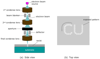

Unlike traditional photolithography that uses light, EBL employs a focused electron beam to draw custom shapes on a surface coated with an electron-sensitive resist.
How Does EBL Work?
Coating the Substrate: A thin layer of electron-sensitive resist material is applied to the substrate (usually a silicon wafer).
Exposure: A finely focused electron beam scans the surface according to a predefined pattern. The electrons alter the chemical structure of the resist in exposed areas.
Development: The exposed resist is developed using a chemical solution, washing away either the exposed or unexposed regions depending on whether a positive or negative resist is used.
Etching or Deposition: The pattern left on the resist serves as a mask for subsequent processes such as etching or material deposition to create the final nanostructure.
Resist Removal: Finally, the remaining resist is removed, leaving behind the desired pattern on the substrate.
Advantages of EBL
High Resolution: Capable of creating features as small as a few nanometers.
Maskless Process: Patterns are written directly, allowing for rapid prototyping and customization.
Flexibility:
Suitable for a wide range of materials and complex designs.
Limitations of EBL
Slow Throughput: Because it writes patterns point-by-point, it is slower than photolithography.
Expensive Equipment:
Requires sophisticated and costly electron beam systems.
Charging Effects: Insulating substrates can accumulate charge, affecting pattern accuracy.
Future of EBL Lithography
The future of Electron Beam Lithography is promising, with ongoing advancements aimed at overcoming its limitations and expanding its applications:
Speed Improvements:
New multi-beam EBL systems are being developed to increase throughput by simultaneously writing multiple patterns.
Integration with AI: Artificial intelligence and machine learning are being explored to optimize pattern writing and reduce errors.
Nanofabrication Advances: EBL continues to be crucial for research in quantum computing, photonics, and biosensors, enabling fabrication at the atomic scale.
Hybrid Techniques: Combining EBL with other lithography methods to balance speed and resolution.
Electron Beam Lithography remains an essential tool in nanofabrication, enabling innovations that push the boundaries of technology. As research continues, EBL will likely become faster, more efficient, and even more integral to the future of electronics and materials science.

https://shorturl.fm/YQuqC